


 BOM
BOM Cart
Cart Product Catalog
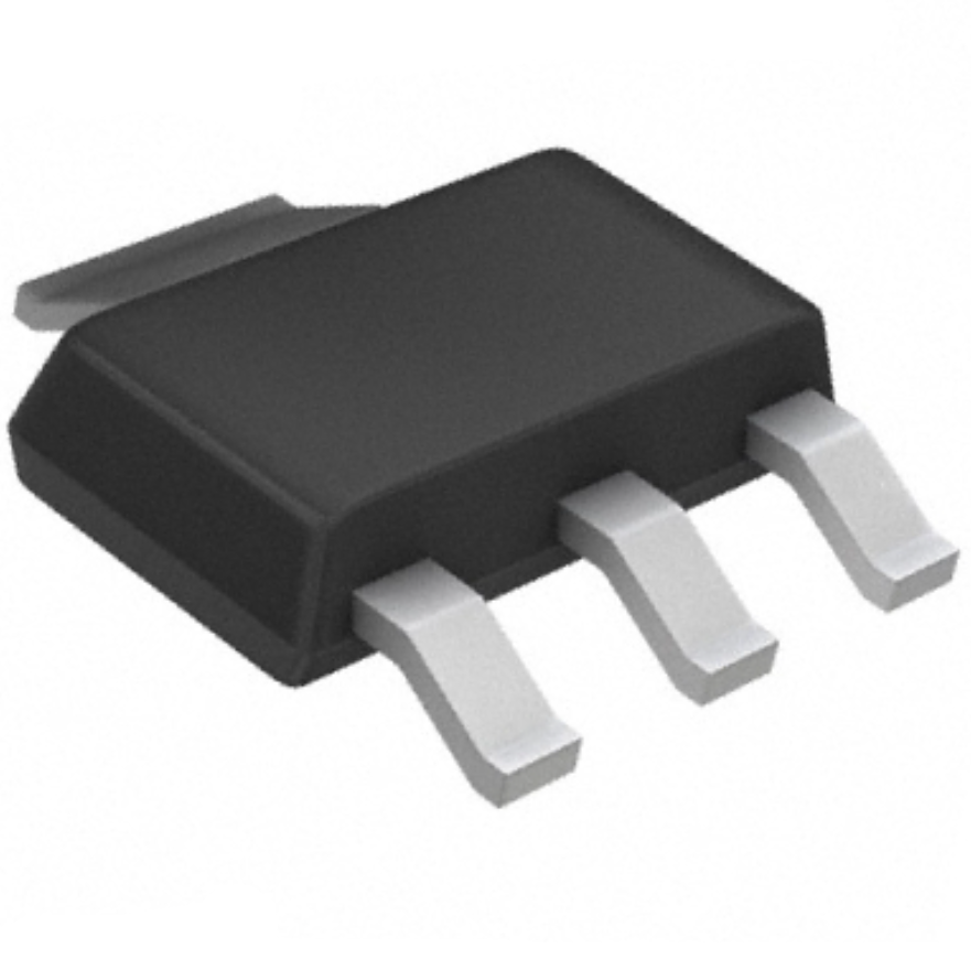
The AO3400 is a powerful and efficient N-Channel MOSFET (Metal-Oxide-Semiconductor Field-Effect Transistor) use in various electronic applications, particularly those requiring low power dissipation and high efficiency. With its advanced trench MOSFET technology and low RDS(ON), the circuit is a popular choice for engineers working on power electronics, portable devices, and DC/DC converters. In this blog post, we’ll dive into the details of the AO3400, here is the catalog:
2. AO3400 Datasheet Technical Specifications
3. CAD Model Design, Package Dimensions, and Pin Configuration of The AO3400 Circuit
4. Working Principle of The AO3400 Mosfet
5. Typical Circuit Applications of the AO3400
6. AO3400 Price, Characteristics and Features
9. Frequently Asked Questions [FAQ]
1. Introduction to the AO3400
The AO3400 is a cutting-edge N-Channel MOSFET designed to offer exceptional performance in low-voltage and high-efficiency applications. Utilizing advanced trench MOSFET technology, this device achieves extremely low RDS(ON), making it an ideal choice for systems where energy efficiency is necessary. Whether you are designing a load switch for portable devices or working on PWM applications, the AO3400 provides a reliable and compact solution to your needs.
Its low resistance characteristics reduce power loss, making it suitable for applications that require efficient power management, especially in portable or battery-powered devices.
2. AO3400 Datasheet Technical Specifications
A compact N-channel MOSFET design for efficient switching and power management applications. Here's a breakdown of its key specs:
Type: N-Channel Enhancement Mode MOSFET
VDS (Drain-Source Voltage): 30V, suitable for low-voltage applications.
Continuous Drain Current (ID): 5.8A (with a gate-source voltage of 10V), meaning it can handle moderate current flow.
Maximum Power Dissipation: 1.5W, which is a limit on how much power the MOSFET can dissipate as heat before it risks damage.
Operating Temperature Range: -50°C to +150°C, allowing it to use in a wide range of temperatures.
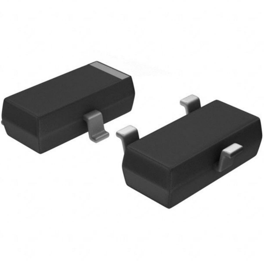
Package: SOT-23, which is a small surface-mount package. It has 3 pads for simple integration into circuits.
RDS(ON): (at VGS=10V) < 28mΩ. (at VGS = 4.5V) < 33mΩ. (at VGS = 2.5V) < 52mΩ, indicating the MOSFET's efficiency drops slightly as gate voltage decreases.
Package Availability: Tape and reel packaging for automated assembly.
This MOSFET is commonly use in low-power switching applications like battery-powered devices, load switching, or power conversion systems, where low RDS(ON) minimizes heat generation and energy loss.
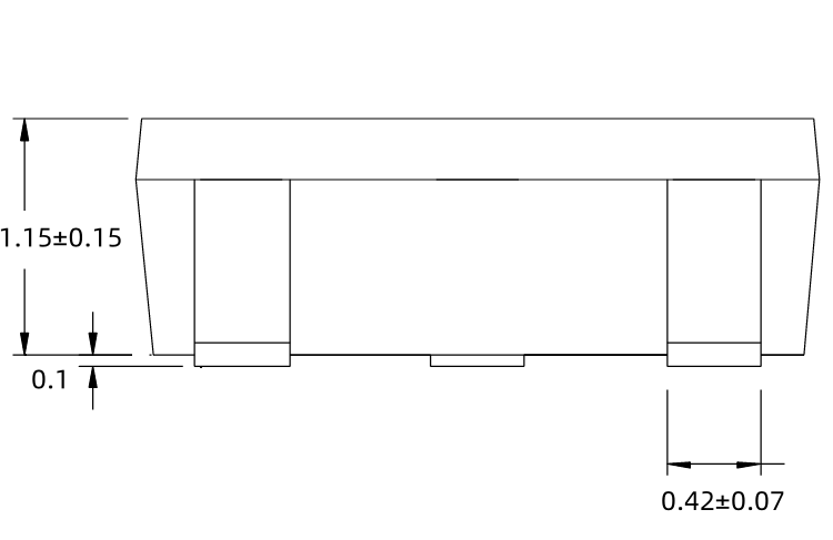
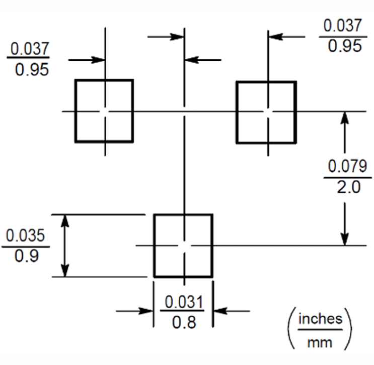
3. CAD Model Design, Package Dimensions, and Pin Configuration of The AO3400 Circuit
The circuit comes in the compact SOT-23 package, which is common for surface-mount devices. The package dimensions and pin configuration are:
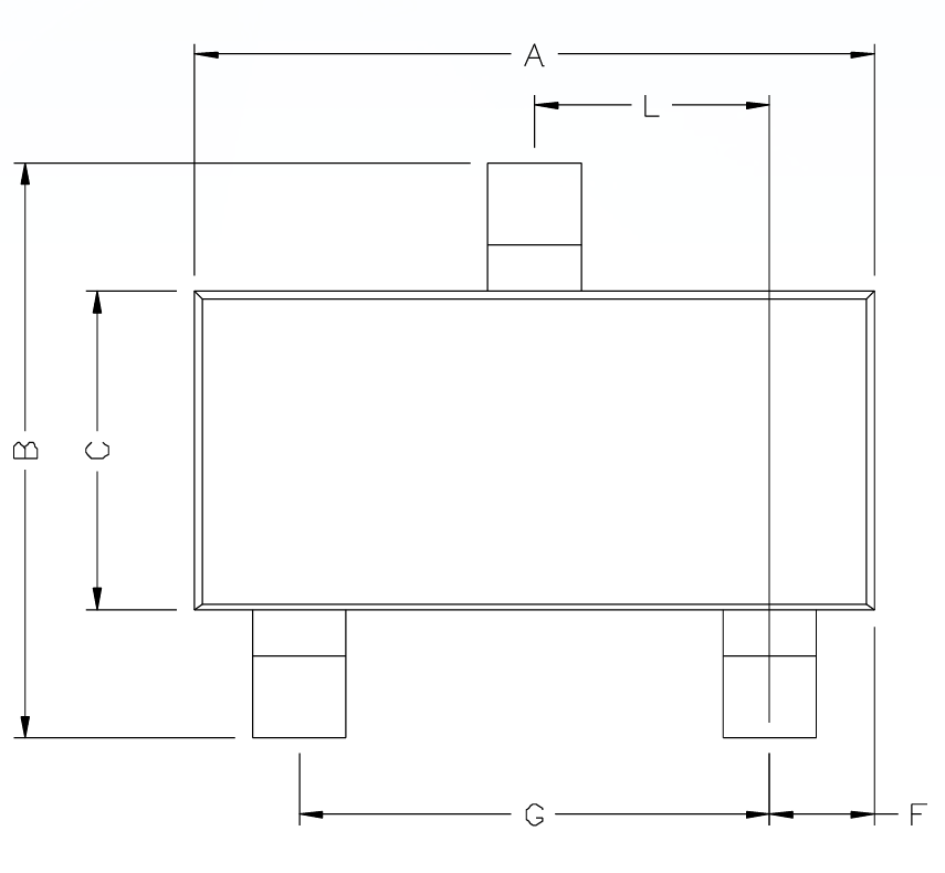
UNIT | A | B | C | L | F | G |
mm | 2.70 3.10 | 2.65 2.95 | 1.50 1.70 | 0.85 1.15 | 0.45 0.55 | 1.9 |
These compact dimensions make it ideal for space-constrained designs while still offering high current-handling capabilities.
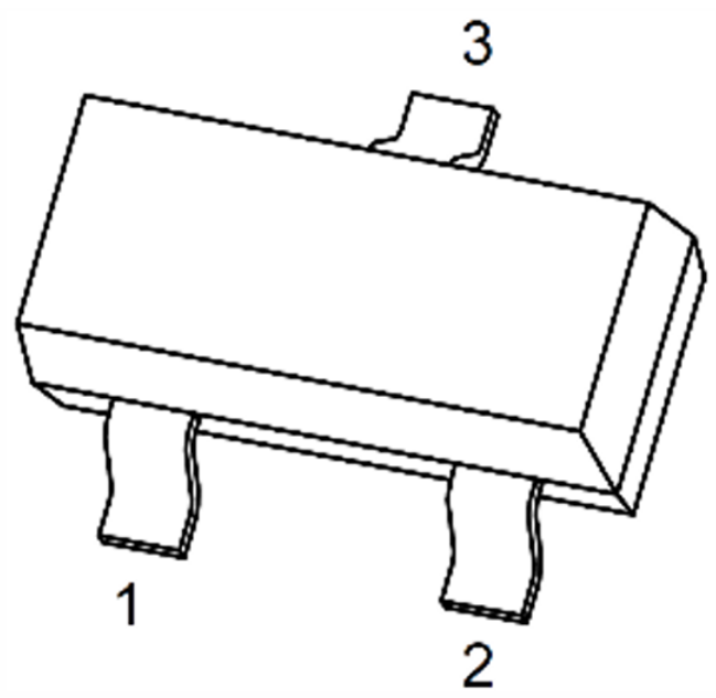
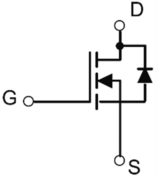
Pin Configuration:
Pin 1: Gate (G) – Controls the switching behavior of the MOSFET.
Pin 2: Source (S) – The terminal through which the current enters the MOSFET.
Pin 3: Drain (D) – The terminal through which the current flows out of the MOSFET.
This standard pinout is typical for N-channel MOSFETs in the SOT-23 package, and it allows for easy integration into most PCB designs for switching and power management applications.
4. Working Principle of The AO3400 Mosfet
The circuit is an N-channel enhancement-mode MOSFET, which means it turns "on" when apply a positive voltage to the Gate relative to the Source. Here’s a more detailed explanation of how it works:
1. Gate (Pin 1):
The Gate (G) controls the operation of the MOSFET. Apply a positive voltage to the gate relative to the Source creates an electric field that attracts electrons to form a conductive channel between the Source and Drain. This channel allows current to flow from the Drain to the Source.
The Gate voltage (VGS) determines the degree of conductivity between the Drain and Source. If the gate voltage is greater than the threshold voltage (Vth), the MOSFET turns on, creating a low-resistance path between the Drain and Source. If the voltage is lower than Vth, the channel does not form, and the MOSFET remains "off," blocking current.
2. Source (Pin 2):
The Source (S) is where the current enters the MOSFET when it is conducting. In an N-channel MOSFET, the Source is typically connected to ground or the negative terminal of the power supply.
Current from the Source control by the voltage applied at the Gate, with the Drain acting as the exit point for the current.
3. Drain (Pin 3):
The Drain (D) is the terminal through which the current flows out of the MOSFET when it is on. For the MOSFET to conduct, the Gate must be positively biased relative to the Source, allowing current to flow from the Drain to the Source.
The amount of current flowing through the Drain is dependent on the Gate voltage and the resistance (RDS(ON)) between the Drain and Source when the MOSFET is fully turned on.
Working Principle:
When VGS > Vth (threshold voltage), an electric field forms a conductive channel between the Drain and Source, allowing current to flow from the Drain to the Source.
The RDS(ON) is the drain-source resistance when the MOSFET is on. In the case of the AO3400, RDS(ON) is low, typically around 28mΩ at VGS = 10V, which ensures low power loss and efficient switching during operation.
The Gate acts as a voltage-controlled switch, meaning that no significant current flows into the Gate, only voltage. This makes MOSFETs efficient, as they require little power to operate.
The MOSFET is capable of 5.8A continuous drain current (ID) at VGS = 10V, making it useful for applications that require efficient current handling.
5. Typical Circuit Applications of the AO3400
The circuit with its low RDS(ON) and efficient switching characteristics, is ideal for various applications, particularly where small size, low power consumption, and fast switching are important. Here are some typical applications:
1. Power Switching Circuits
Load Switches: Can use to control power delivery to a load. It can turn on or off the power supply to a specific section of a circuit with minimal voltage drop and heat generation.
Example: Power management in battery-powered devices where switching efficiency is important to extend battery life.
2. Level Shifting and Logic Circuits
Level Shifters: The AO3400 can use in circuits that require translating logic levels between different voltage domains, such as interfacing 3.3V logic with 5V systems.
Example: Logic signal interface between microcontrollers and peripherals with different voltage levels.
3. Battery-Powered Systems
Power Control for Battery-Powered Devices: The low RDS(ON) makes it ideal for managing the power in portable devices like smartphones, tablets, and other battery-operated gadgets.
Example: Power rail switching in a mobile device, where it can efficiently control the power from the battery to various internal circuits.
4. DC-DC Converters
Switching in DC-DC Conversion: Used in the switch-mode power supplies (SMPS) circuits like buck, boost, or buck-boost converters.
Example: In a buck converter (step-down voltage regulator), the MOSFET can be used to switch the input voltage on and off rapidly to control the output voltage.
6. AO3400 Price, Characteristics and Features
The MOSFET is typically priced in the low-cost range because its small form factor and widespread use in consumer and low-power applications. The price can vary depending on factors like: Quantity purchased (bulk orders typically reduce the per-unit cost). Distributor or retailer pricing. Package type (e.g., tape-and-reel packaging).
As of typical market prices, the AO3400 generally costs around $0.01 to $0.30 USD per unit for small orders (a few pieces). For bulk purchases (thousands), the price can drop significantly, sometimes under $0.005 per unit. Always check with specific distributors for the most up-to-date prices.
Characteristics and Features (Advantages & Disadvantages)
Advantages:
1.Low RDS(ON) Values:
With 28mΩ (at VGS = 10V), it minimizes the power loss during operation, making it highly efficient, particularly for high-speed switching.
This characteristic is particularly beneficial for battery-powered systems and power converters where energy efficiency is necessary.
2.Compact Package (SOT-23):
The small packing size makes it ideal for space-constrained applications like mobile devices and portable electronics.
It can fit easily into small PCBs, making it ideal for dense circuit designs.
3.High Current Handling (5.8A at VGS = 10V):
Can handle moderate to high currents (5.8A), making it suitable for power management in a range of devices like DC-DC converters, LED drivers, and motor controllers.
4.Low Gate Drive Voltage (VGS > 1V):
The MOSFET can be driven with relatively low gate voltages, making it compatible with low-voltage logic signals, useful for interfacing with microcontrollers and other low-voltage systems.
5.Wide Operating Temperature Range (-50°C to +150°C):
The AO3400's wide temperature tolerance makes it suitable for automotive applications, industrial environments, and extreme-temperature settings.
6.Fast Switching Speed:
The circuit features low gate charge, which allows for fast switching. This makes it highly suitable for high-frequency switching applications like SMPS and PWM control.
7.Affordability:
Its cost-effective pricing makes it an excellent choice for cost-sensitive applications while still providing reliable performance.
Disadvantages:
1.Limited Maximum Voltage (30V):
The 30V maximum drain-source voltage limits its use in high-voltage applications. For circuits needing higher voltage tolerance (such as power supplies for industrial systems), other MOSFETs with higher VDS ratings would be more suitable.
2.Relatively Low Power Dissipation (1.5W):
While 1.5W is sufficient for many low-power applications, higher-power circuits may require MOSFETs with higher power dissipation ratings, especially in heavy load conditions.
3.Higher RDS(ON) at Lower Gate Voltages:
As the gate-source voltage (VGS) decreases, the RDS(ON) increases (e.g., 52mΩ at VGS = 2.5V). This leads to higher power loss at lower gate drive voltages, making the MOSFET less efficient in circuits where the gate voltage is low.
4.Small Package Size:
The SOT-23 package is small, which may not be ideal for circuits requiring heat dissipation or higher current handling, where larger packages like DPAK or TO-220 would be more appropriate.
5.Not Suitable for High Current Applications:
With a continuous drain current of 5.8A, the AO3400 is suitable for low to moderate current applications, but for too high-current circuits, a MOSFET with a higher current rating would be necessary.
6.Limited Gate Drive Voltage Range:
The maximum VGS of 10V is common for many MOSFETs, but in applications requiring higher gate voltages for better conduction, the AO3400 may not be ideal.
7. AO3400 Equivalent
Comparison table:
Part Number | VDS (Drain-Source Voltage) | ID (Drain Current) | RDS(ON) |
AO3400 | 30V | 5.8A | 28mΩ |
AOSS32334C | 30V | 5A | 25mΩ |
PJA3400_R1_00001 | 30V | 5A | 35mΩ |
PMV20ENR | 20V | 5.2A | 75mΩ |
SI3404-TP | 30V | 4A | 40mΩ |
AO3400: Low RDS(ON), efficient for low-voltage applications.
AOSS32334C: Lower RDS(ON) than AO3400, similar performance.
PJA3400_R1_00001: Higher RDS(ON) than AO3400, suitable for cost-sensitive apps.
PMV20ENR: Lower VDS and higher RDS(ON), less efficient for high-speed switching.
SI3404-TP:Higher RDS(ON) than AO3400, but suitable for low-power applications.
8. Manufacturer Overview
The circuit manufacture by Alpha & Omega Semiconductor Inc. (AOS), a leading supplier of advanced power semiconductors. AOS focuses on providing high-performance solutions for power management applications. Their product portfolio includes MOSFETs, diodes, and other power management devices, used in a wide range of industries from consumer electronics to automotive and industrial systems.
Other manufacturers like MDD, EVVO, and UMW may also produce similar MOSFETs, but AOS remains the primary producer of the AO3400.
9. Frequently Asked Questions [FAQ]
1. What is the max current of AO3400?
The maximum current the AO3400 can handle is 5.8A when the gate-source voltage (VGS) is 10V. This allows it to perform well in applications requiring moderate current flow, like power switching and load control. Higher current ratings make it ideal for low-voltage, high-efficiency circuits, ensuring minimal power loss and heat dissipation during operation.
2. How does an n channel MOSFET work?
An N-channel MOSFET controls current between the drain and source terminals. When apply a positive voltage (VGS) to the gate, it creates a conductive channel between drain and source, allowing current to flow. The MOSFET turns on when VGS exceeds the threshold voltage (Vth), and it turns off when VGS is below Vth. The current flow depends on the gate voltage and the resistance (RDS(ON)) between drain and source.
3. How to check MOSFET with multimeter?
To check a MOSFET with a multimeter, set it to diode mode. For an N-channel MOSFET, test the gate to source and drain to source. A good MOSFET shows a diode drop (0.7V) from gate to source in one direction and a small voltage drop (0.2–0.3V) from drain to source. In reverse, the multimeter should show no continuity. A faulty MOSFET will show no voltage drop or continuity in the expected directions.
4. What packaging types are available for the AO3400?
The AO3400 MOSFET is available in the SOT-23 package, a compact surface-mount package. It typically has 3 pins and is designed for space-constrained applications. The package is often available in tape-and-reel packaging, which is suitable for automated PCB assembly. The SOT-23 package is commonly use in low-power circuits, ensuring efficient switching with minimal footprint.
5. What are common applications for the AO3400?
Use in various low-voltage power management applications, such as DC-DC converters, load switches, and LED drivers. Ideal for battery-powered devices, logic level switching, and motor control circuits because its low RDS(ON), compact size, and efficient switching characteristics. The MOSFET's low power dissipation makes it particularly useful in portable electronics like smartphones and wearables.
6. What is the working principle of a FET?
A Field-Effect Transistor (FET) works by controlling the flow of current between two terminals (drain and source) with an electric field created by the gate terminal. In an N-channel FET, applying a voltage (VGS) to the gate induces a conductive channel between drain and source, allowing current to flow. The FET operates as a voltage-controlled device, where the gate voltage determines whether the transistor is on or off, regulating current flow. The FET’s resistance between the drain and control source by the gate voltage.
Conclusion
The AO3400 is a highly efficient and reliable N-Channel MOSFET, making it a popular choice for engineers working on low-power, high-efficiency applications. With its low RDS(ON), high current handling, and compact size, it serves as a perfect solution for portable devices, DC/DC converters, and other power management systems. Whether you're designing a new project or replacing an older component, the component offers the performance and features needed to meet your power requirements.
Read More:
1. Understanding the TXD2-3V Relay-Features-Applications-and Selection Guide
HOT NEWS
Understanding A 0603 Resistor
0603 resistor,dimensions,marking code, values
2025-05-29
The 0402 Resistor: A Comprehensive Guide
0402 Resistor
2025-05-06
LR41 Battery Guide: Specifications, Equivalents, and Uses
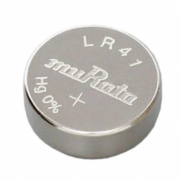
LR41 Battery Specifications, Equivalents, and Uses
2025-12-14
MT3608 Boost Converter - An In-Depth Guide
MT3608 Boost Converter
2025-09-04
What Is A 1206 Resistor?
1206 resistor dimensions,footprint,value
2025-06-05
TP4056 Charging Module Pinout, Working, and Applications
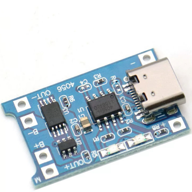
TP4056 Charging Module Pinout, Working, and Applications
2026-01-23
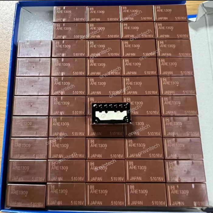
Everything You Need To Know About ARE1309 Relay
2025-04-23
Complete Guide to the 220 Ohm Resistor
220 Ohm Resistor
2025-07-28
120 Ohm Resistor- Specifications, Applications, and Features
2025-05-12
Guide To The AMS1117 Voltage Regulator
AMS1117 Voltage Regulator Circuit
2025-08-17