




 BOM
 Cart
 Product Catalog
The 74LS08 is a popular digital logic IC designed for basic AND gate operations in electronic circuits. It contains four independent 2-input AND gates in a single 14-pin package, making it useful for combining multiple logic signals without requiring several individual ICs. Based on Low-Power Schottky TTL technology, this chip offers a good balance between switching speed and power consumption.
The device operates with a 5V power supply and commonly use in digital systems, control circuits, signal processing, and logic-level decision-making applications. This guide covers the 74LS08 pinout, features, electrical specifications, working principles, practical usage, and common applications.
3. Quadruple Two Input AND Gate Features
8. Frequently Asked Questions [FAQ]
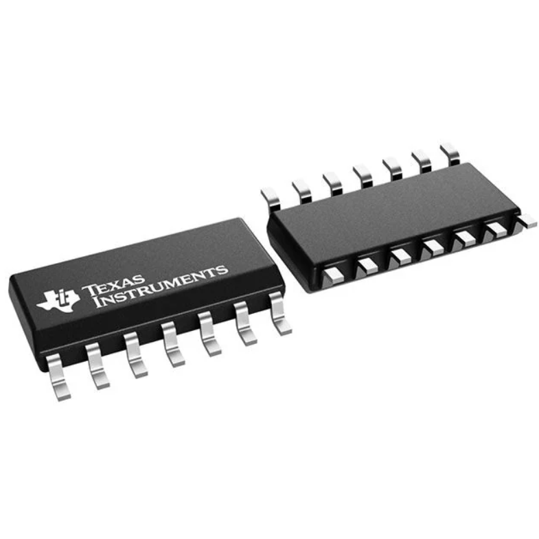
What is 74LS08?
The 74LS08 is a quadruple 2-input AND gate integrated circuit belonging to the 74LS series of Low-Power Schottky TTL logic devices. It contains four independent AND gates, with each gate having two inputs and one output.
An AND gate produces a HIGH output only when both input signals are HIGH. If either input is LOW, the output remains LOW. This simple logic function makes the device useful for implementing logical conditions in digital electronic systems.
The IC operates with a nominal 5V power supply and uses TTL-compatible input and output logic levels. Its four independent gates allow designers to perform multiple AND operations within a single package, helping reduce circuit size and component count.
The 74LS08 is available in different package types, including DIP and SOIC. The SN7408, SN74LS08, and SN74S08 versions are characterized for operation from 0°C to 70°C, while their SN54-series counterparts are designed for the wider military temperature range of -55°C to 125°C.
74LS08 Pinout
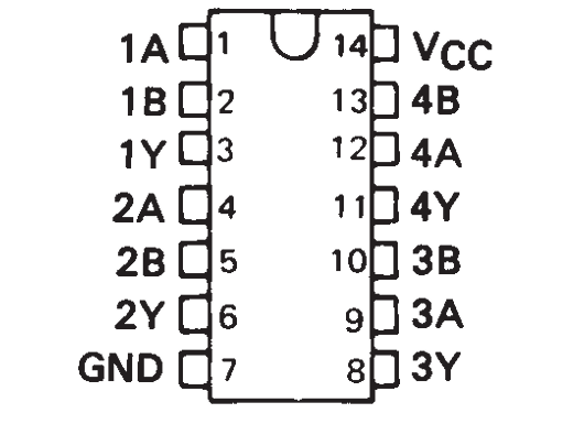
The 74LS08 comes in a 14-pin package containing four independent AND gates. Each gate has two input pins and one output pin. Pin 7 is connected to ground, while pin 14 supplies the operating voltage.
74LS08 Pin Configuration
Pin Number | Pin Name | Description |
1 | 1A | First input of AND gate 1 |
2 | 1B | Second input of AND gate 1 |
3 | 1Y | Output of AND gate 1 |
4 | 2A | First input of AND gate 2 |
5 | 2B | Second input of AND gate 2 |
6 | 2Y | Output of AND gate 2 |
7 | GND | Ground connection |
8 | 3Y | Output of AND gate 3 |
9 | 3A | First input of AND gate 3 |
10 | 3B | Second input of AND gate 3 |
11 | 4Y | Output of AND gate 4 |
12 | 4A | First input of AND gate 4 |
13 | 4B | Second input of AND gate 4 |
14 | VCC | Positive power supply |
74LS08 Logic Truth Table
Each of the four AND gates follows the same Boolean logic function:
[ Y=Acdot B ]
Input A | Input B | Output Y |
LOW (0) | LOW (0) | LOW (0) |
LOW (0) | HIGH (1) | LOW (0) |
HIGH (1) | LOW (0) | LOW (0) |
HIGH (1) | HIGH (1) | HIGH (1) |
The output becomes HIGH only when both inputs are HIGH. This behavior allows the IC to control digital operations based on two simultaneous conditions.
Quadruple Two-Input AND Gate Features
The 74LS08 is a quadruple 2-input AND gate IC designed for digital logic applications. It integrates four independent AND gates into a single 14-pin package, allowing multiple logic operations without requiring additional ICs.
Its main features include:
Four Independent AND Gates: Contains four separate AND gates that can operate independently.
Two Inputs per Gate: Each gate has two input pins and one output pin.
Low-Power Schottky Technology: Provides a balance between low power consumption and high switching speed.
5V Power Supply: Operates with a recommended supply voltage of 4.75V~5.25V.
Fast Switching: Provides a maximum propagation delay of approximately 20 ns under the specified test conditions.
TTL Logic Compatibility: Supports standard TTL-compatible digital logic levels.
Compact Package: Available in 14-pin DIP and SOIC package options, depending on the manufacturer.
Wide Applications: Suitable for digital control circuits, signal gating, logic processing, and microcontroller-based projects.
Other important features include independent gate operation, straightforward TTL compatibility, relatively low power consumption, and the ability to perform multiple logic operations using a single chip.
74LS08 Specifications
The following table summarizes the main electrical and packaging specifications of the 74 LS08 based on the supplied component information.
Parameter | Value |
Manufacturer | Texas Instruments |
Series | 74LS |
Logic Type | AND Gate |
Number of Circuits | 4 |
Number of Inputs | 2 per gate |
Supply Voltage | 4.75V~5.25V |
Output Current (HIGH) | 400 µA |
Output Current (LOW) | 8 mA |
Input Logic Level (LOW) | 0.8V maximum |
Input Logic Level (HIGH) | 2V minimum |
Maximum Propagation Delay | 20 ns @ 5V, 15 pF |
Operating Temperature | 0°C~70°C |
Mounting Type | Surface Mount |
Package | 14-SOIC |
Packaging | Tape & Reel (TR) |
Base Product Number | 74LS08 |
Note: The electrical limits and propagation delay depend on the specific manufacturer and device variant. Always check the corresponding datasheet when designing a circuit.
How to use a 74LS08 IC?
The 74LS08 is easy to use in basic digital logic circuits. It requires a regulated 5V power supply and two digital input signals for each AND gate. The output changes according to the logic levels applied to its inputs.
Basic Circuit Connections
To use the first AND gate, follow these connections:
1. Connect pin 14 (VCC) to the positive 5V power supply.
2. Connect pin 7 (GND) to the power supply ground.
3. Connect pin 1 (1A) to the first digital input signal.
4. Connect pin 2 (1B) to the second digital input signal.
5. Connect pin 3 (1Y) to the output circuit, such as an LED indicator through a suitable current-limiting resistor.
When both input pins receive HIGH signals, the output at pin 3 becomes HIGH. If either input is LOW, the output becomes LOW.
Connecting with a Microcontroller
The IC can also work with microcontrollers such as Arduino and other 5V-compatible digital systems. Two GPIO pins can provide the input signals, while another GPIO input can monitor the AND gate output.
For example, the output becomes HIGH only when two control signals are activated simultaneously. This arrangement can be used for simple condition checking, digital signal combination, and hardware-based control logic.
Important: The 74LS 08 uses TTL input thresholds. When connecting it to 3.3V logic systems, check the input and output voltage compatibility. Avoid leaving unused inputs floating; connect them to defined HIGH or LOW logic levels. Also recommend a 100 nF decoupling capacitor between VCC and GND.
Where to use 74LS08 Chip?
The 74LS 08 is suitable for digital electronic systems that require multiple AND logic operations. Since it contains four separate gates, it can handle several independent input conditions without additional logic ICs.
It is particularly useful in circuits where an output should be activated only when two specific conditions are satisfied. For example, a control system require both an enable signal and a sensor signal to be HIGH before allowing an operation.
The chip can also be integrated into microcontroller interfaces, digital communication circuits, timing systems, and basic computer logic designs. Its standard 74LS-series logic compatibility makes it convenient for educational projects, prototyping, and traditional TTL-based circuits.
74LS08 Applications
The 74LS08 is widely used in digital electronics because it provides four independent AND gates in a compact package. Common applications include:
Digital Logic Circuits: Combines two binary input signals to generate an output based on AND logic. It is useful for building more complex combinational logic circuits.
Control Systems: Checks multiple control conditions before activating a particular function. For example, a machine can be enabled only when both the start and safety signals are HIGH.
Microcontroller Projects: Works with compatible digital control signals from Arduino, development boards, and other embedded systems.
Signal Gating: Allows a digital signal to pass through a logic operation only when the required enable condition is satisfied.
Alarm and Security Systems: Combines sensor signals and activation conditions to control alarm outputs.
Computer and Digital Systems: Supports basic arithmetic control, data processing, address decoding, and other digital logic operations.
Educational Projects: Helps students understand Boolean algebra, AND gate operation, truth tables, and combinational logic design.
Frequently Asked Questions [FAQ]
What is the maximum supply voltage for a 74LS08?
The recommended operating supply voltage for the 74LS08 is 4.75V to 5.25V, with 5V as the nominal value. Do not exceed the manufacturer's absolute maximum ratings. Recommend a regulated 5V supply for reliable operation in standard TTL circuits.
What is the delay time for 74LS08?
The maximum propagation delay specified in the supplied specifications is approximately 20 ns at 5V with a 15 pF load capacitance. Actual switching time depends on operating conditions, load capacitance, temperature, and the manufacturer's particular device version.
What is price of 74LS08?
The price of the 74LS08 depends on the manufacturer, package type, purchase quantity, and supplier. Standard DIP and surface-mount versions have different prices. For an accurate quotation, check current electronic component distributors or contact your preferred component supplier.
How many AND gates are inside a 74LS08?
The 74LS08 contains four independent 2-input AND gates. Each gate has two input pins and one output pin, allowing the IC to perform four separate AND logic operations simultaneously.
Is 74LS08 compatible with Arduino?
The 74LS 08 can interface with Arduino boards that provide compatible 5V TTL logic signals. For 3.3V Arduino-compatible boards, check the input thresholds and output voltage requirements before connecting the devices directly.
What is the difference between 7408 and 74LS08?
Both devices contain four independent 2-input AND gates. The main difference is their logic technology. The 7408 uses standard TTL technology, while the 74LS08 uses Low-Power Schottky TTL technology, offering lower power consumption and different switching characteristics.
Conclusion
The 74LS08 is a practical quadruple 2-input AND gate IC for digital logic applications. With four independent gates, a standard 5V supply, and straightforward pin configuration, it provides a simple way to combine multiple digital signals in one package.
Whether used in educational experiments, microcontroller projects, control systems, or combinational logic circuits, this device remains a useful component for basic TTL-based designs. Before implementation, check the datasheet for electrical limits, timing characteristics, and package-specific information to ensure reliable operation.
Read More:
1. TTP223 Touch Switch - Pinout, Datasheet & Applications
2. LR41 Battery Guide: Specifications, Equivalents, and Uses
HOT NEWS
TP4056 Charging Module Pinout, Working, and Applications
TP4056 Charging Module Pinout, Working, and Applications
2026-01-23
LR41 Battery Guide: Specifications, Equivalents, and Uses
LR41 Battery Specifications, Equivalents, and Uses
2025-12-14
Understanding The CD4051 Analog Multiplexer
CD4051 analog multiplexer
2025-06-30
Understanding A 0603 Resistor
0603 resistor,dimensions,marking code, values
2025-05-29
MT3608 Boost Converter - An In-Depth Guide
MT3608 Boost Converter
2025-09-04
The 0402 Resistor: A Comprehensive Guide
0402 Resistor
2025-05-06
Complete Guide to the 220 Ohm Resistor
220 Ohm Resistor
2025-07-28
Mini MP1584 DC-DC 3A Buck Converter Module: Complete Guide
Mini MP1584 DC-DC 3A Buck Converter Module: Complete Guide
2026-03-26
Guide To The XL6009 Boost Converter
XL6009 Boost Converter
2025-09-05
What Is A 1206 Resistor?
1206 resistor dimensions,footprint,value
2025-06-05